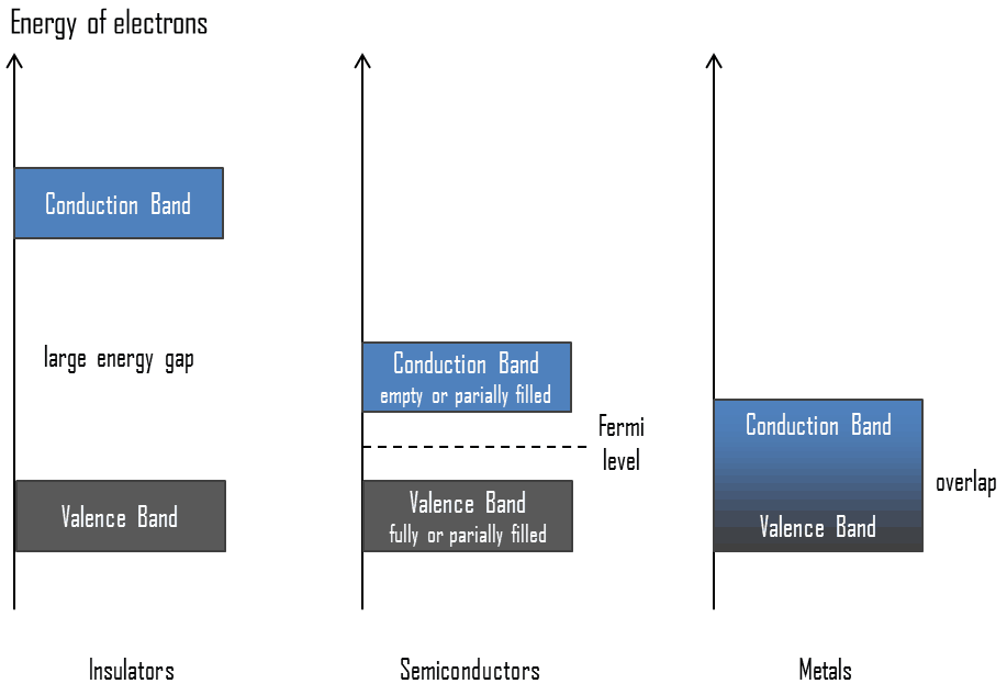
Fermi Level In Semiconductor / Fermi Levels And Quasi Fermi Levels Of Electrons And Holes For An Download Scientific Diagram - The band theory of solids gives the picture that there is a sizable gap between the fermi level and the conduction band of the semiconductor.
Fermi Level In Semiconductor / Fermi Levels And Quasi Fermi Levels Of Electrons And Holes For An Download Scientific Diagram - The band theory of solids gives the picture that there is a sizable gap between the fermi level and the conduction band of the semiconductor.. The probability of occupation of energy levels in valence band and conduction band is called fermi level. I cant get the plot. Uniform electric field on uniform sample 2. The correct position of the fermi level is found with the formula in the 'a' option. We hope, this article, fermi level in semiconductors, helps you.
Where will be the position of the fermi. Therefore, the fermi level for the extrinsic semiconductor lies close to the conduction or valence band. Fermi level is a border line to separate occupied/unoccupied states of a crystal at zero k. The band theory of solids gives the picture that there is a sizable gap between the fermi level and the conduction band of the semiconductor. (ii) fermi energy level :
What Is Fermi Level In Semiconductors Definition from material-properties.org Fermi level is also defined as the. The fermi level (i.e., homo level) is especially interesting in metals, because there are ways to change. It is a thermodynamic quantity usually denoted by µ or ef for brevity. As the temperature increases free electrons and holes gets generated. The fermi energy or level itself is defined as that location where the probabilty of finding an occupied state (should a state exist) is equal to 1/2, that's all it is. Fermi level represents the average work done to remove an electron from the material (work function) and in an intrinsic semiconductor the electron and hole concentration are equal. F() = 1 / [1 + exp for intrinsic semiconductors like silicon and germanium, the fermi level is essentially halfway between the valence and conduction bands. We hope, this article, fermi level in semiconductors, helps you.
The fermi level is the surface of fermi sea at absolute zero where no electrons will have enough energy to rise above the surface.
Thus, electrons have to be accommodated at higher energy levels. (ii) fermi energy level : Ne = number of electrons in conduction band. As the temperature increases free electrons and holes gets generated. Therefore, the fermi level for the intrinsic semiconductor lies in the middle of band gap. at any temperature t > 0k. Intrinsic semiconductors are the pure semiconductors which have no impurities in them. The fermi level is on the order of electron volts (e.g., 7 ev for copper), whereas the thermal energy kt is only about 0.026 ev at 300k. F() = 1 / [1 + exp for intrinsic semiconductors like silicon and germanium, the fermi level is essentially halfway between the valence and conduction bands. We hope, this article, fermi level in semiconductors, helps you. Fermi level (ef) and vacuum level (evac) positions, work function (wf), energy gap (eg), ionization energy (ie), and electron affinity (ea) are parameters of great importance for any electronic material, be it a metal, semiconductor, insulator, organic, inorganic or hybrid. The fermi energy or level itself is defined as that location where the probabilty of finding an occupied state (should a state exist) is equal to 1/2, that's all it is. Where will be the position of the fermi.
at any temperature t > 0k. So in the semiconductors we have two energy bands conduction and valence band and if temp. It is well estblished for metallic systems. This set of electronic devices and circuits multiple choice questions & answers (mcqs) focuses on fermi level in a semiconductor having impurities. • the fermi function and the fermi level.
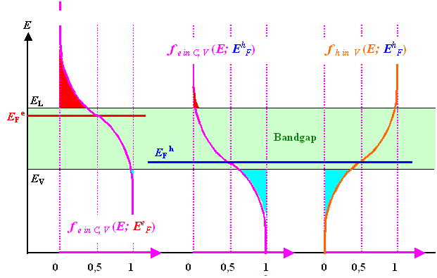
Gate Ese Effect Of Doping In P Type Semiconductor Fermi Energy In Hindi Offered By Unacademy from edge.uacdn.net Fermi level represents the average work done to remove an electron from the material (work function) and in an intrinsic semiconductor the electron and hole concentration are equal. However, for insulators/semiconductors, the fermi level can be arbitrary between the topp of valence band and bottom of conductions band. A quasi fermi level (also called imref, which is fermi spelled backwards) is a term used in quantum mechanics and especially in solid state physics for the fermi level (chemical potential of electrons) that describes the population of electrons separately in the conduction band and valence band. Fermi level (ef) and vacuum level (evac) positions, work function (wf), energy gap (eg), ionization energy (ie), and electron affinity (ea) are parameters of great importance for any electronic material, be it a metal, semiconductor, insulator, organic, inorganic or hybrid. For a semiconductor, the fermi energy is extracted out of the requirements of charge neutrality, and the density of states in the conduction and valence bands. Uniform electric field on uniform sample 2. Where will be the position of the fermi. Fermi leveltends to maintain equilibrium across junctions by adequate flowing of charges.
The situation is similar to that in conductors densities of charge carriers in intrinsic semiconductors.
The fermi level is on the order of electron volts (e.g., 7 ev for copper), whereas the thermal energy kt is only about 0.026 ev at 300k. Uniform electric field on uniform sample 2. Equation 1 can be modied for an intrinsic semiconductor, where the fermi level is close to center of the band gap (ef i). The fermi level is on the order of electron volts (e.g., 7 ev for copper), whereas the thermal energy kt is only about 0.026 ev at 300k. Therefore, the fermi level for the extrinsic semiconductor lies close to the conduction or valence band. Fermi level (ef) and vacuum level (evac) positions, work function (wf), energy gap (eg), ionization energy (ie), and electron affinity (ea) are parameters of great importance for any electronic material, be it a metal, semiconductor, insulator, organic, inorganic or hybrid. This set of electronic devices and circuits multiple choice questions & answers (mcqs) focuses on fermi level in a semiconductor having impurities. The band theory of solids gives the picture that there is a sizable gap between the fermi level and the conduction band of the semiconductor. Www.studyleague.com 2 semiconductor fermilevel in intrinsic and extrinsic. Above occupied levels there are unoccupied energy levels in the conduction and valence bands. at any temperature t > 0k. Fermi level is also defined as the. Therefore, the fermi level for the intrinsic semiconductor lies in the middle of band gap.
It is a thermodynamic quantity usually denoted by µ or ef for brevity. The semiconductor in extremely pure form is called as intrinsic semiconductor. Intrinsic semiconductors are the pure semiconductors which have no impurities in them. Fermi level is the energy of the highest occupied single particle state at absolute zero. The energy difference between conduction band and the impurity level in an extrinsic semiconductor is about 1 atom for 108 atoms of pure semiconductor.
2 3 2 Quasi Fermi Energies from www.tf.uni-kiel.de It is well estblished for metallic systems. The fermi level is on the order of electron volts (e.g., 7 ev for copper), whereas the thermal energy kt is only about 0.026 ev at 300k. The fermi level is the surface of fermi sea at absolute zero where no electrons will have enough energy to rise above the surface. Ne = number of electrons in conduction band. Fermi level is also defined as the. The illustration below shows the implications of the fermi function for the electrical conductivity of a semiconductor. If so, give us a like in the sidebar. I cant get the plot.
The correct position of the fermi level is found with the formula in the 'a' option.
The occupancy of semiconductor energy levels. at any temperature t > 0k. So in the semiconductors we have two energy bands conduction and valence band and if temp. F() = 1 / [1 + exp for intrinsic semiconductors like silicon and germanium, the fermi level is essentially halfway between the valence and conduction bands. Fermi level is also defined as the. Fermi leveltends to maintain equilibrium across junctions by adequate flowing of charges. To a large extent, these parameters. A quasi fermi level (also called imref, which is fermi spelled backwards) is a term used in quantum mechanics and especially in solid state physics for the fermi level (chemical potential of electrons) that describes the population of electrons separately in the conduction band and valence band. Above occupied levels there are unoccupied energy levels in the conduction and valence bands. Increases the fermi level should increase, is that. Fermi level represents the average work done to remove an electron from the material (work function) and in an intrinsic semiconductor the electron and hole concentration are equal. The illustration below shows the implications of the fermi function for the electrical conductivity of a semiconductor. It is a thermodynamic quantity usually denoted by µ or ef for brevity.


0 Komentar